UV Imaging as a Non-Destructive QA Tool for Ceramic Insulators in Semiconductor Manufacturing
< Back to Articles & Case Studies
High-voltage ceramic insulators used in vacuum and ultra-high-voltage environments are required to perform under extreme electrical stress.
While conventional electrical tests may confirm basic insulation integrity, they often fail to reveal surface-related phenomena that can later lead to instability, performance degradation, or unexpected breakdown events.
Recent field evaluations demonstrated that high-sensitivity UV imaging can reveal optical activity generated by electrical discharges on ceramic insulators that remains invisible to standard electrical measurement tools — providing additional insight into insulation behavior under real operating conditions.
CHALLENGE — WHEN STANDARD TESTS ARE NOT ENOUGH
In systems such as electron optics and high-voltage vacuum assemblies, ceramic insulators must maintain stable electrical behavior under strong electric field gradients.
In practice, manufacturers and system integrators often encounter:
- Batch-to-batch variability in ceramic components
- Inconsistent performance despite identical electrical test results
- Failures or instability appearing only under real operational stress
Two insulators may pass conventional resistance or leakage tests, yet behave very differently once installed in high-voltage systems.
The challenge is identifying potential risk before integration into costly or mission-critical equipment.
VISUAL OBSERVATIONS — FIELD EVALUATION
During a recent high-voltage evaluation, ceramic (alumina-based) insulators were monitored using a solar-blind UV imaging system.
The UV inspection revealed clear differences in optical behavior between components subjected to identical electrical conditions.
Observation 1: Optical Activity Under HV Stress
- Some insulators remained optically dark during operation
- Others exhibited localized UV emissions along the ceramic surface
These emissions appeared prior to any visible arc or electrical failure and were not detectable by standard instrumentation.
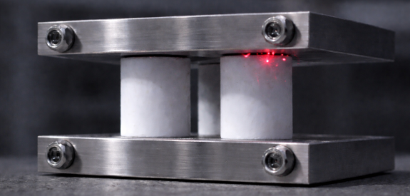
Illustrative representation of discharge activity detection
Observation 2: Residual Optical Emissions After De-Energization
In a separate observation, faint UV activity was detected on an insulator that had not been energized for an extended period.
Although conventional measurements indicated no remaining voltage, the UV camera identified persistent low-level optical signals originating from the ceramic surface.
WHAT UV IMAGING ADDS
Rather than replacing electrical tests, UV imaging provides an additional diagnostic layer:
- Visualization of surface-related discharge activity under real HV stress
- Early indication of components that behave differently despite identical specifications
- Non-contact, non-destructive inspection suitable for QA and R&D environments
These observations enable engineers to compare components, designs, and material batches using direct visual evidence, rather than relying solely on pass/fail electrical thresholds.
POTENTIAL APPLICATIONS
Integrating UV imaging into high-voltage testing workflows can support:
- Incoming inspection of ceramic batches
Identifying parts that exhibit abnormal discharge behavior under stress - Design and material evaluation
Comparing insulator geometries, coatings, or manufacturing processes - Failure analysis support
Adding visual context to recurring or unexplained HV issues