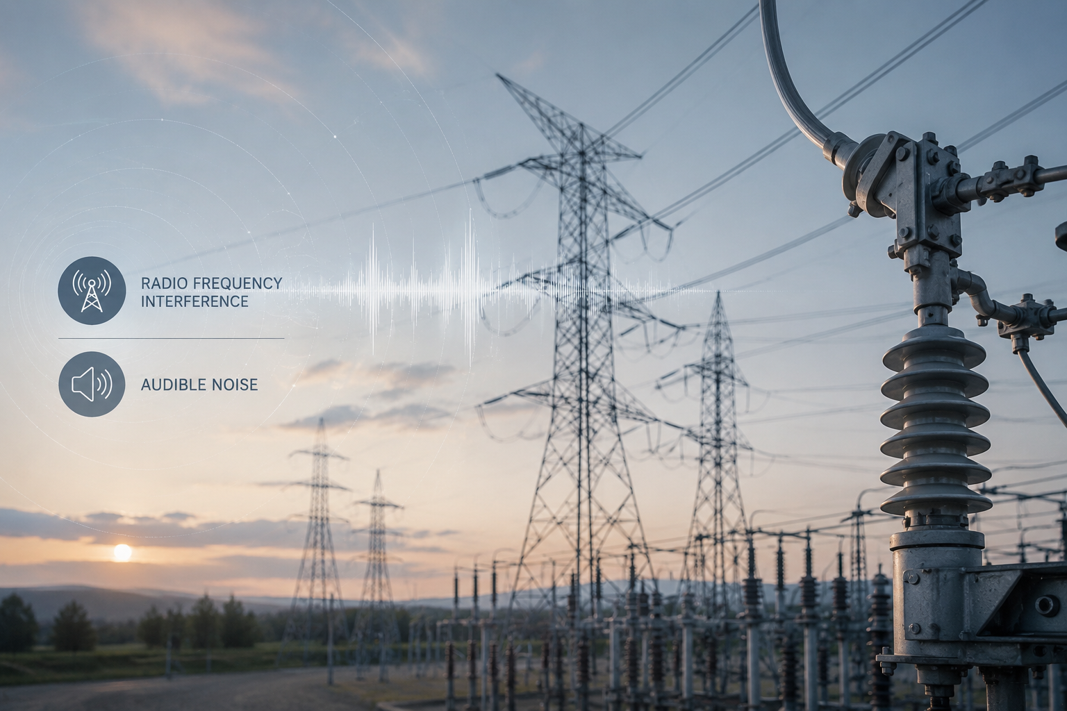
Radio Frequency Interference (RFI) and Audible Noise: Hidden Consequences of Corona PD Activity
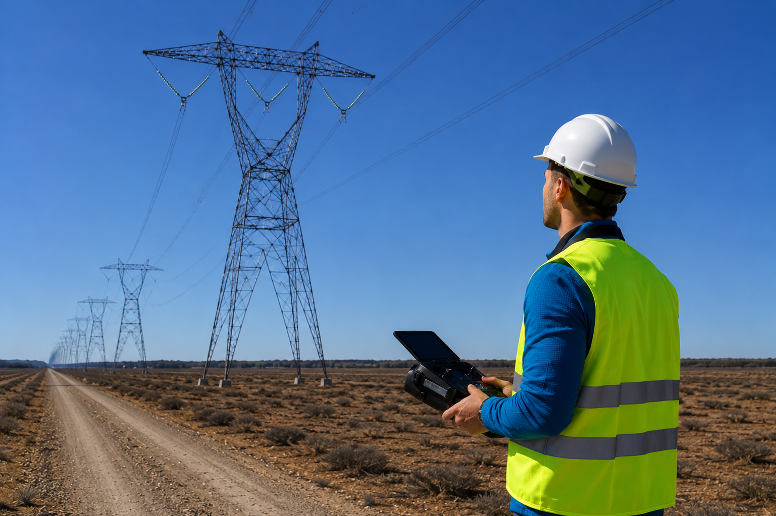
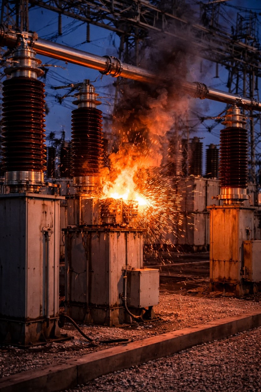
Corona partial discharge affects more than equipment reliability. It can generate radio frequency interference and audible noise that disrupt communications, trigger regulatory concerns, and generate customer complaints. This article explains why early detection is essential for reliable grid operation.